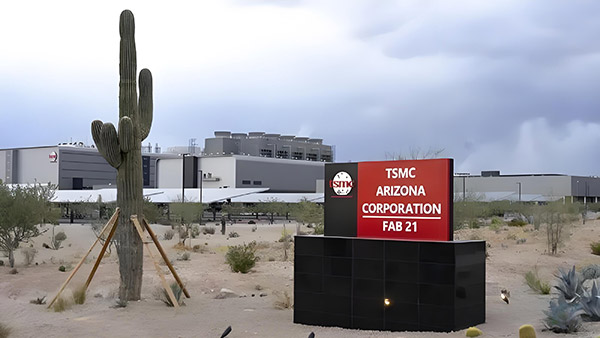
TSMC launches construction of its third wafer fab in Arizona, accelerating expansion of production layout in the United States
2025-05-06
According to Bloomberg, as the Trump administration plans to impose tariffs on semiconductors, TSMC has started construction on its third wafer fab in Arizona to accelerate its expansion in the United States.
TSMC previously announced a $65 billion investment in the construction of three wafer fabs, including the first phase's 4nm wafer fab, which began mass production at the end of last year; The second phase 3nm wafer fab was originally scheduled to start mass production in 2026, but was later postponed to 2028; The third phase wafer fab will produce 2nm or more advanced process technology, with the original plan to mass produce between 2029 and 2030.
However, previous rumors have shown that in response to the requirements of major customers such as AMD and Apple, TSMC originally planned to carry out the P2A installation plan for its second plant in Arizona in the fourth quarter of 2026. However, the supplier has been notified that it will start and install in September this year, and the production time is expected to be advanced by at least two quarters.
The latest report from Bloomberg shows that TSMC's third wafer fab in Arizona has also started construction ahead of schedule, and the production time is expected to be advanced. TSMC's move is mainly in response to Apple AMD、 Customers such as NVIDIA, Qualcomm, and Broadcom have strong demand for AI, and the third wafer fab is expected to mass produce 2nm and A16 processes.
It is worth noting that the start of construction for TSMC's third wafer fab in Arizona coincided with the inspection of TSMC's Arizona base by US Secretary of Commerce Howard Lutnick.
TSMC also stated that its Arizona wafer fab is the largest single foreign direct investment case in US history, and welcomes Lutnik's visit. TSMC Arizona CEO Yinglang Wang and General Manager Rose Castanares received Lutnik and showed him the progress of the Arizona plant operations.
In March of this year, TSMC Executive Chairman and President Wei Zhe jia appeared at the White House with US President Trump and announced an additional investment of $100 billion in the United States to enhance domestic production capacity. This expenditure is an additional addition to the originally planned $65 billion investment, with plans to build three new wafer fabs, two advanced packaging fabs, and one research and development center.
According to the information disclosed by Wei Zhejia at the previous press conference, after the investment in wafer fab projects in the United States is in place, TSMC will have about 30% of its cutting-edge process capacity below 2nm located in Arizona, forming an independent advanced manufacturing cluster in the United States, creating greater economies of scale, and helping to cultivate a more complete semiconductor supply chain ecosystem in the United States. This will also enable TSMC to continue playing a crucial and indispensable role in helping customers achieve success. While continuing to be a key partner, we can also fully leverage all the advantages and leadership positions of the US semiconductor industry.


 Karmin Electronic (HK) Limited
  Hong Kong Tel:852-39070580 96557277
 Hong Kong Fax:852-39070581
 Email:
 Hong Kong address: Room 6, 11th floor, Huali industrial center, 10 - 14guidi street, Fo Tan, New Territories, Hong Kong